Here I begin assembling the Tecsun 2p3 AM radio, which I told you about in this previous post.
The Tecsun 2p3 has unusual instructions. They come on one sheet, approximately 20″ x 30″. It’s about the size of eight sheets of notebook paper. It’s not a booklet, but more of a two-sided poster. There is plenty of information there, but no step-by-step guide to construction.
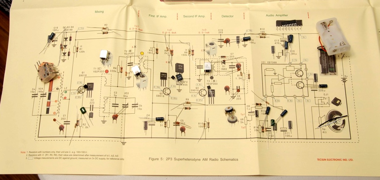
A part of the guide is the schematic, above. It’s very large and detailed, with photographs of the components next to their schematic symbols. I used the schematic as a guide to inventory the parts, making sure I could identify each one, and place it on its proper place in the schematic. Then, to populate the board, I just took parts off of the schematic and soldered them onto the board until all the parts were transferred.
The order of the installations of parts isn’t critical. I started by going left to right across the schematic, but didn’t stick to that order very strictly. I soldered around two or three components in at a time, then trimmed the leads, and flipped the board over for another round. You may use my order as a guide, or choose your own path.
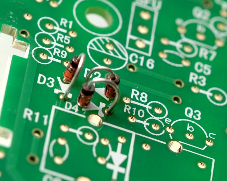
Diodes D2, D3, and D4. Be careful about the orientation of the black bands on the diodes.
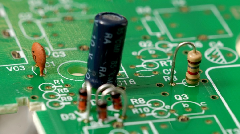
Capacitors C1 and C16, and resistor R3. Notice I always place the gold tolerance bands of resistors at the bottom, next to the board. The electrons don’t care at all which way you insert resistors, but I find it easier to have a consistent orientation in case I have to go back and check my work. Besides, it looks nicer.
Resistor R2 and Transistor Q1.
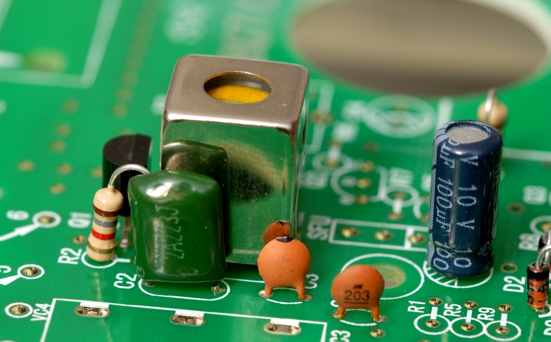
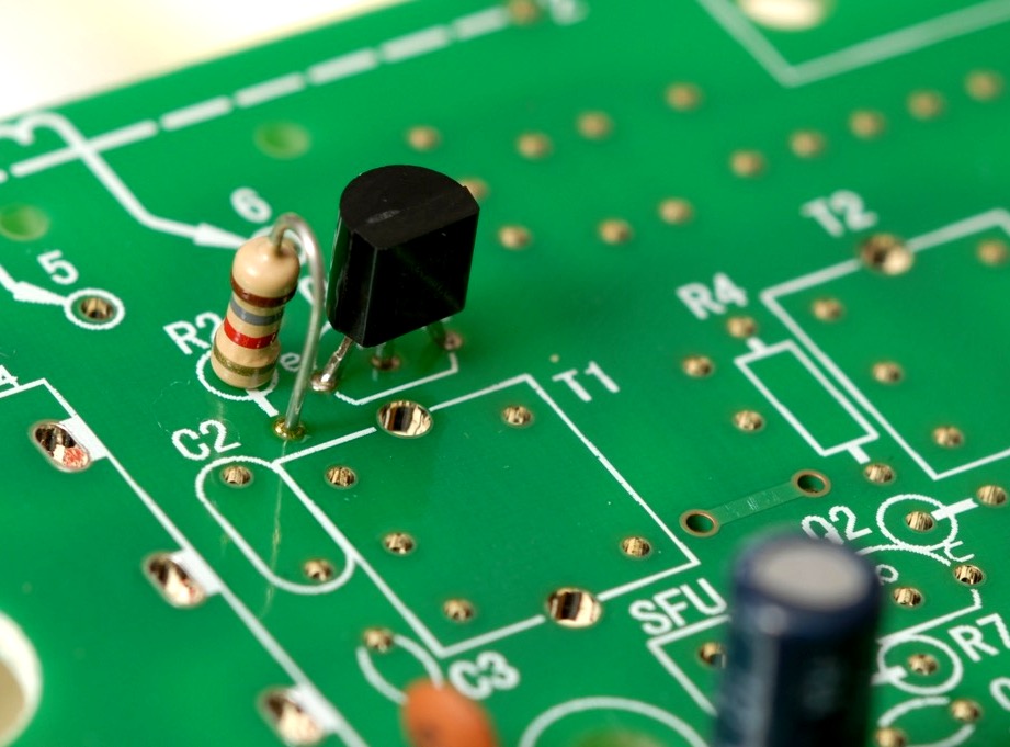
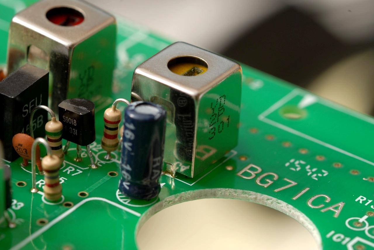
Transformer T1, capacitors C2 and C3. Notice that transformer T1 looks a lot like T2. But T1 has a red screw on the top, unlike the one in this photo (oops). Transformers are hard to remove, once installed. Guess how I know. Be sure and double-check to get yours correct, according to the instructions, and don’t use this photo as a guide.
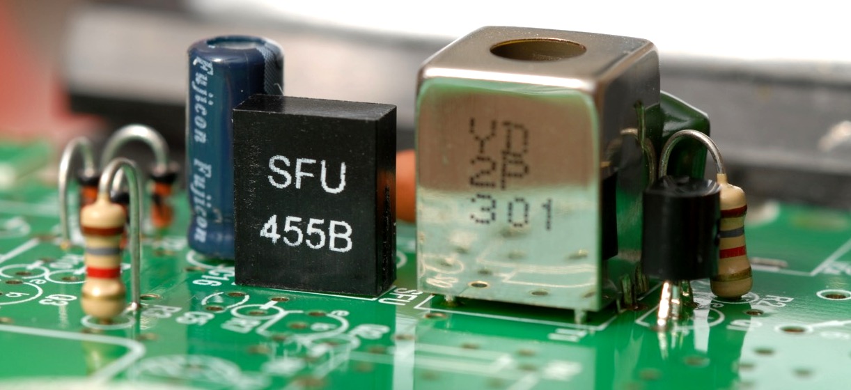
Ceramic filter SFU455
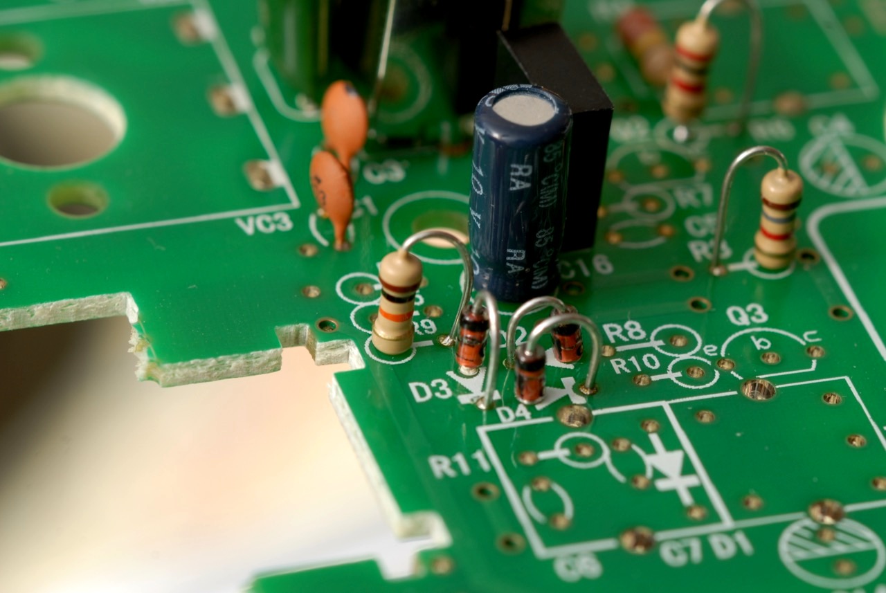
Resistor R9. The schematic tells us that the values for resistors R1, R5, and R8 are determined after measuring lc1, lc2, and lc3. So I decided not to insert those resistors at first. But later, I realized you have to insert the nominal valued resistors for R1, R5, and R8 to start, then take the measurements, and if needed, remove the original resistors and insert slightly different values. So I could have inserted R1 and R5 at this time. Oh well.
I also inserted R4 and R6, but they’re not in focus in this shot. You can see them better in the next photo.
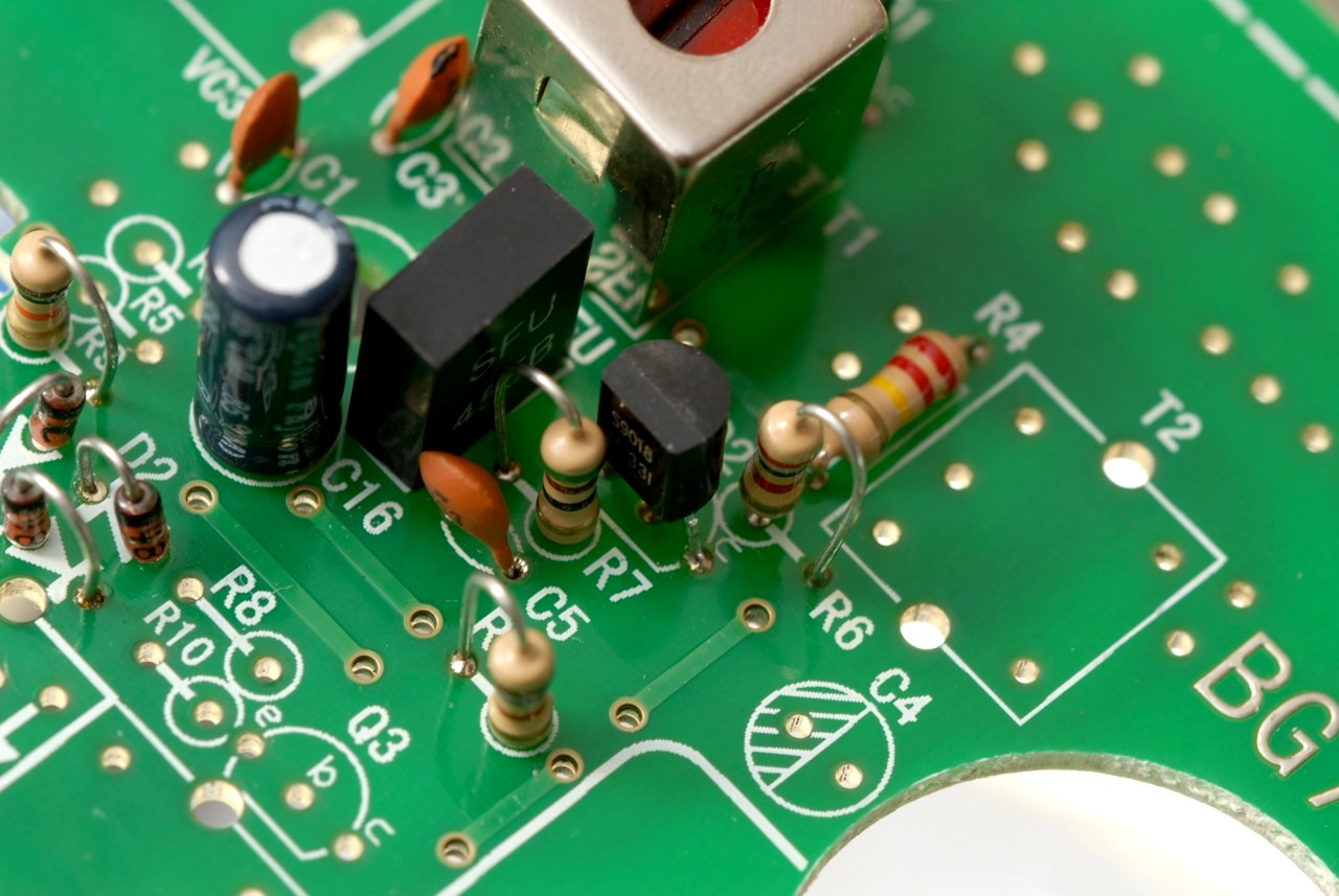
Q2, R7, and C5. Also, you can see R4 and R6 from the previous step.
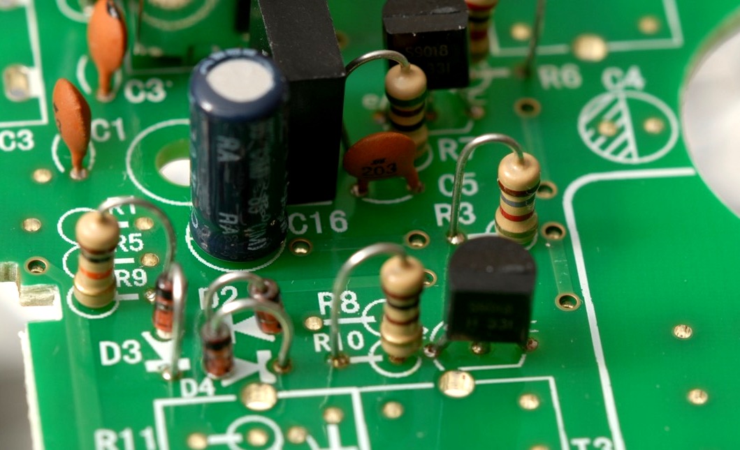
R10 and Q3.
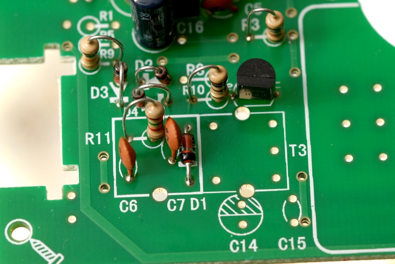
C6, R11, C7, and D1.
T3.
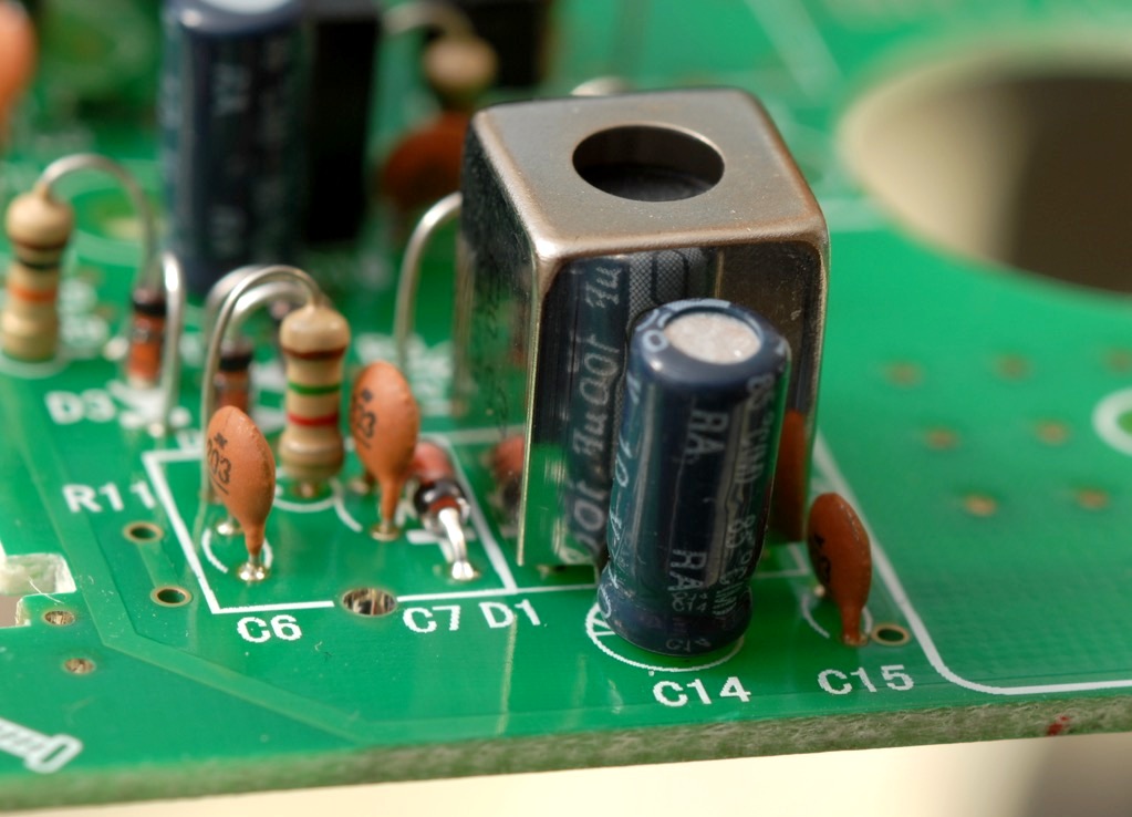
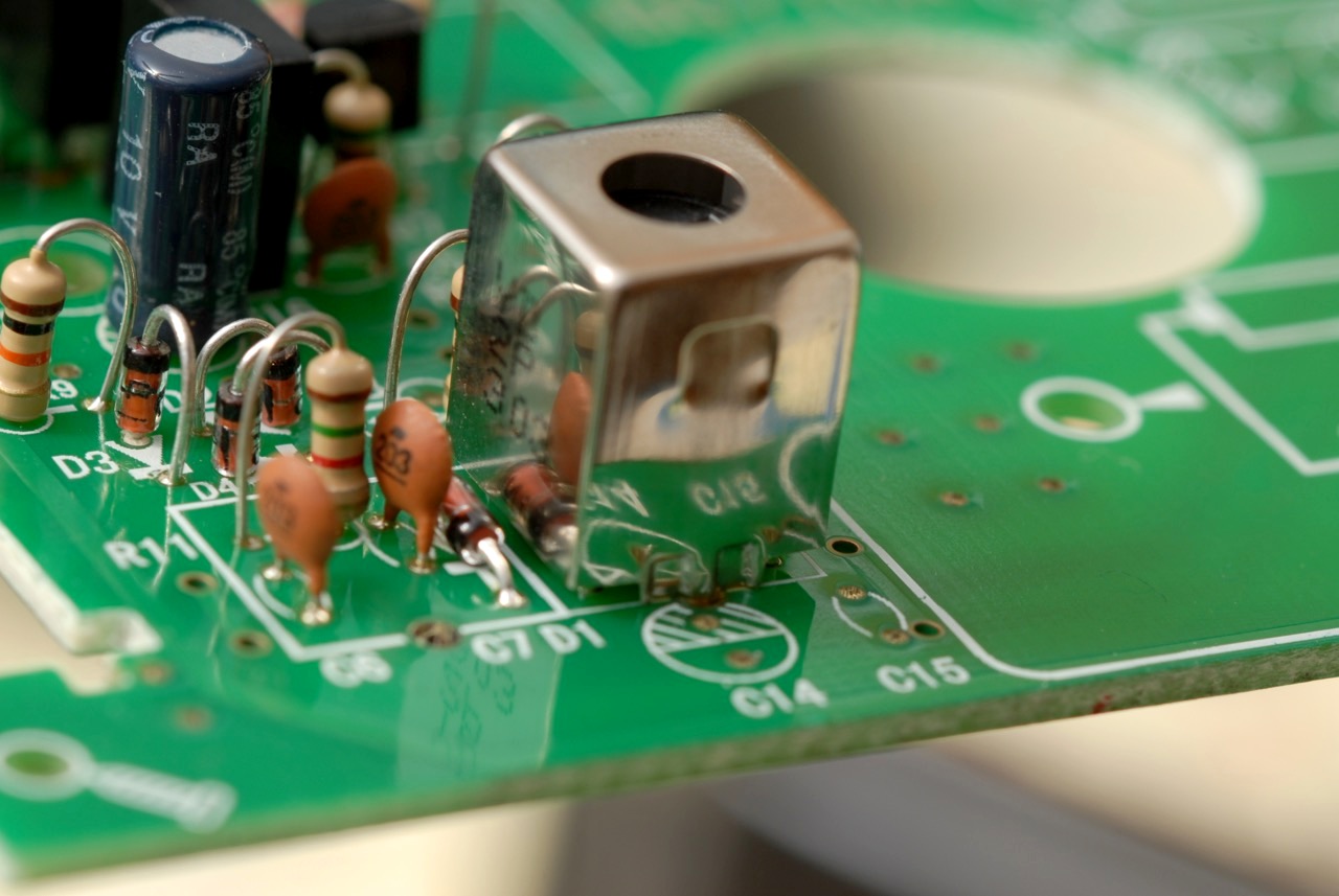
C14 and C15.
T2 and C4. Note the correct colors on T1 and T2 now.
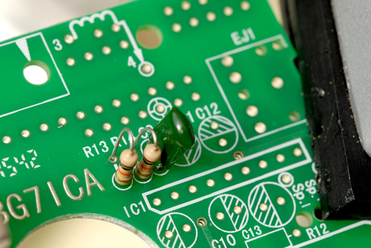
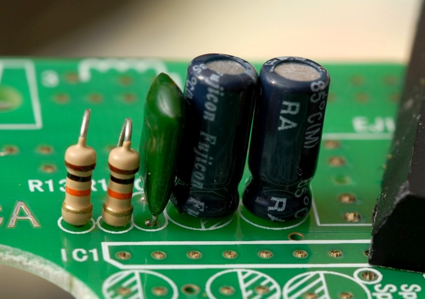
R13, R14, and C9.
C11 and C12.
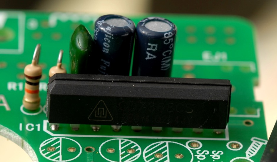
IC1. To solder a multi-pin IC like this, I first lightly tack solder one pin at one end. Then I press and hold the IC in place while melting the joint to make sure the pin is fully inserted. Then repeat the process at the other end, lightly tacking it in place and pressing it into the board while heating the joint. Then I inspect and make sure the IC is exactly where I want it. Finally, I solder all the middle pins, and re-heat the pins on the end to make sure they are well-soldered with no mechanical stress.
Time to pause for a break now. Stay tuned for more…